Now ASICs are beginning to overtake cryptocurrency mining on GPUs (video cards), ASICs are being released for new and new algorithms. However, an alternative to ASICs and GPUs has emerged.
Today we will talk about programmable logic integrated circuit or FPGA for short.
These electronic elements combine what we love most about graphics cards and ASICs.
The only problem is that there are very few of these boards available today, and if you want to get into FPGA mining, you have to do it... now.
Why is FPGA interesting for mining?
Watch the video:
subscribe
What is fpga
FPGA stands for Field Programmable Gate Array, which in Russian translates as “field programmable gate array”, abbreviated to FPGA.
It is a type of FPGA - programmable logic integrated system. The microcircuit is a semiconductor. Used in cases where the device is designed to perform logical operations such as and, or, nand and others.
That is, it is a microcircuit with repeating logical blocks connected in a circuit. They can be configured at your own discretion, taking into account the tasks.
FPGA mining spread at one time, since the task of mining is to perform the same type of operations. This was the first step before ASICs.
But during mining, the temperature of the device rose too much, cooling and providing electricity became costly, reducing the profitability of the fpga miner.
Device manufacturers solved the problem by improving ergonomics, stability and temperature.
FPGAs, even in chain mode, act as one miner (UART port). When the board is connected to a PC, it is recognized as a ttyUSB or COM device under Windows.
The normal error rate is less than 0.1%, if the error rate increases, it means something has gone wrong.
The FPGA requires an additional fan. Temperature sensing allows cgminer to shut down the FPGA if it gets too hot.
Trigger.
FPGAs use programmable D flip-flops. When configuring, you can set such trigger operating modes as a trigger with initial reset (R) or initial installation (S), with recording on the edge or fall of a synchronization series, with or without recording permission.
After configuration is complete, the FPGA issues a general reset signal GSR, which sets all flip-flops to 0 or 1.
Mining on fpga Altera
This device can still be considered top-end in terms of performance. Produced along with Spartan (one of the first).
In late 2011 and early 2012, innovative companies such as Butterfly Labs and ZTEX began offering FPGA-based mining devices. Most of them were based on Xilinx Spartan6-150 (200 to 220 MH/s) FPGAs costing $100, while the BFL devices used Altera (830 MH/s), which the company received at a reduced price.
But the price for the miner was still high, $600 per chip.
In mid-2012, BFL began shipping a so-called miniRig 25.2 GH/s device, consisting of a case and fans, with several boards inside (usually 17-18) for a total hash speed of 25.2 GHz/s. Altera's miniRig FPGAs were even more expensive, with the entire design costing $15,000. Then the company smoothly switched to ASIC.
A miner that uses a compatible FPGA board can work in a pool or alone.
The first open source FPGA project Bitcoin mine was released on May 20, 2011 for Altera and Xilinx FPGAs. To compile the code, you need at least basic technical knowledge.
People used the chips to mine BTC, LTC, DOGE and other coins. All FPGA designs were most often SHA256 or Scrypt. The community created a scheme for X11 mining. ASICs began to displace these miners.
KLB structure.
In the basic XC4000 FPGA series from Xilinx, the main unit of equipment is considered to be a CLB, consisting of two flip-flops and two LTs. In the new series of FPGAs, the number of triggers and LTs has doubled and quadrupled. In order to leave the same piece of equipment for all series, we agreed to call a CLB consisting of two triggers and two LTs an equivalent CLB (ECLB) or CLB slice. Thus, the Virtex series CLB consists of two ECLBs, and the VirtexII series - of four ECLBs.
FPGA vs ASIC
The first thing to note is that developing an FPGA is much easier. Unlike FPGAs, ASIC design starts with a completely empty table. This does not mean that everyone will set up a chip for mining at home. But if you have a base and read the experience of others (more on this below), the task is theoretically feasible.
On an FPGA you start with a large array of logic blocks, PLLs, on-chip RAMs, I/O buffers, (de)serializers, power distribution networks, etc., ASIC development yourself starts at an even lower level. This means that components must be purchased or manufactured as part of a library, or custom designed for the ASIC.
One ASIC production cycle can take several weeks (months), after which you need to integrate and test it. After testing, bugs are not fixed, it is too expensive.
ASIC technology provides higher speed and lower power consumption compared to FPGA. The differences in speed between the two methods are easily 10 times or more.
Synchronization system.
One of the principles of developing projects for FPGAs is the principle of single-cycle synchronization, according to which all flip-flops in the block are triggered simultaneously by one clock signal. To implement it in an FPGA, clock signals are distributed through a high-speed tree-like network, which ensures the almost simultaneous arrival of the clock pulse front at the clock inputs of all flip-flops.
For reliable operation of the FPGA, the clock signal must be supplied through the GCLKPAD pin and enter the clock series network through the GCLKBUF buffer. The FPGA has 4 GCLKPAD pins located on opposite sides of its body. The clock signal can also be generated inside the FPGA, but in this case it should be connected to the clock series network through the global buffer BUFG.
Using a designed synchronous machine configured in the FPGA, you can change the frequency and phase of the synchronization series. But in this case, its time parameters will not be stable enough and therefore this approach is usually not used. To reliably regulate the clock frequency, the FPGA includes clock series frequency dividers with auto-tuning - CLKDLL blocks. In Fig. A typical diagram of its connection is shown. The CLKDLL block provides multiplication of the clock frequency by 2 times, shifting its phase by 90, 180 and 270 degrees, division by 1.5, 2, 2.5, 3, 4.5, 8 and 16.
Comparison with GPU
GPUs are significantly more powerful than CPU's, both in power and hash/watt, but due to FGPA's inherent parallelism can be around 15x more efficient.
Overall, the takeaway from FPDAs is that they consume less power and can be reconfigured and designed by yourself if you're good with microelectronics. But they have:
Despite the higher price, ASIC will be more profitable. But for coins that are resistant to such development, you can try an FPGA miner.
Ready-made offers on the market
The project plan is as follows:
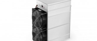
It is also known that the Baikal miner for Criptonight is an FPGA, which is their key advantage after the release of Bitmain Antminer X3. If a coin changes its hashing algorithm, the hardware can be reconfigured.
We cannot recommend specific sites, because the attitude towards the possibility of mining using the cryptonight algorithm on fpga is controversial.
Also, mining programs and other ready-made solutions are usually either paid or take a commission from the mined in the amount of 3–5%.
Source
Is it possible to assemble an ASIC miner with your own hands?
In an attempt to save money, many are looking for ways to assemble an ASIC miner with their own hands and start making money on cryptocurrencies. The motivation lies in the fast-growing market and strong price fluctuations. Everyone has heard about Bitcoin, Ethereum, Ripple, etc. But few people understand how to mine cryptocurrencies and what equipment is needed for this. Let's talk in detail about assembling a car yourself to make money.
Why assemble an ASIC if the market offers ready-made solutions? The main problem with ASICs is their availability. It seems that they looked at a specific model and chose a supplier. All that remains is to order. But as soon as a specific conversation begins, we hear in response: “Sorry, we’ve sorted everything out.”
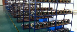
Buying an ASIC is a risk and responsibility that you assume. Buying is not easy, and delivery can bring a lot of inconvenience. But in the event of a breakdown, everything becomes very sad. The equipment must be sent to China (where most ASICs are assembled). This is expensive, plus time losses.
Taking a ready-made option in your city is not profitable from an economic point of view. The payback on equipment will increase significantly. Outbids drive unrealistic prices. Therefore, you will have to order from China or America. Difficulties fuel interest in assembling with your own hands.
Where to begin?
Let's look at a little theory. What is ASIC? This is a specialized machine to solve a specific task. In our case, cryptocurrency mining. The device is complex, but if you try, you can assemble an ASIC miner with your own hands. In this case, the mining of cryptocurrencies will be carried out in exactly the same way as in the case of a ready-made solution.
Using video cards is a safer investment. With their help you can mine almost all known cryptocurrencies. At any time, the video card can be sold on the secondary market. While Asik ties the owner to the industry. If we didn’t manage to sell on time, we lost money. But working with ASICs is a completely different volume.
A specific ASIC model is designed for mining 1-2 cryptocurrencies. This is compensated by enviable performance, which is several times higher than that of a GPU. If ASICS are so good at mining, then why not use only them? Demand for equipment significantly exceeds supply. Prices are 2-3 times higher than the actual cost. Therefore, video cards, ASICs and independent production are used. In general, any means to grab your piece of the pie.
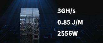
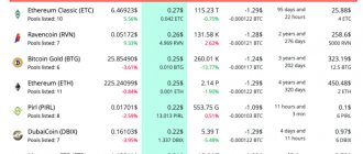
Is 1900 MH/s hashrate fake?
There are rumors on the network that FPGA VCU1525 devices are capable of delivering 1900 MH/s on Ethereum’s Ethash algorithm. Most likely this is a fake.
According to our calculations, one FPGA device cannot produce 1900 MH/s; most likely, a rig of 6 FPGAs gives this figure.
An FPGA can be 10 times more powerful than a video card, but no more.
1900 MH/s would be capable of issuing an ASIC if it could be produced.
Do GPUs pose a threat to FPGA miners?
The device costs around $4,000 and is most likely 10 times more powerful than video cards.
At the same time, the warranty for video cards is usually 3 years, while for FPGA vendors it is only 3 months.
Most likely, the devices are suitable only for large, “industrial” miners. At the moment it is easier to buy video cards, because... the payback is almost the same.
If you can't buy it, do it yourself
The shortage of equipment became the impetus for the emergence of homemade ASIC miners. It will take a lot of time to assemble the miner. But trying is a good experience and an additional opportunity to earn money. Where do we start?
We're not afraid of problems, are we? The main thing is to follow the plan. If you decide to make an ASIC for mining with your own hands or are assembling a farm from video cards, follow the instructions and do not forget about planning. Cryptocurrencies require a quick response; with a clear strategy, you can recoup the costs of purchasing components for an ASIC in a matter of months.
The main advantage of ASICs is performance. The disadvantages are offset by quick payback. At the same time, old models can be successfully sold, recover part of the invested money and have time to mine a net profit.
Self-assembly also entails problems with noise levels. The ASIC will work quite loudly. This is a minus, but we will return to it a little later.
What are the benefits of assembling it yourself?
The ready-made version and the one assembled from components purchased separately have their pros and cons. ASIC from the manufacturer - no hemorrhoids, quick installation and connection. Self-assembly requires a long search for boards, assembly difficulties, time losses. But all the disadvantages are covered by savings. If you get a good offer on the retail market, you can save a lot. This is the main incentive when assembling with your own hands.
In addition, understanding all the intricacies and nuances of Asik’s work is very useful. You can proudly declare that you assembled this ASIC for mining with your own hands. At the same time, everything works and makes a profit. We sorted out the purchase of microcircuits and the search for software. Let's move on to the components.
Ready-made version VS homemade
With the right approach, self-assembly will not cause problems. We wrote a plan in advance. We described it point by point: where we get the components, how the power is supplied, what we do with cooling. The rest is trifles. If you managed to assemble AntMiner with your own hands, then understanding the intricacies of cryptocurrency mining is a mere trifle.
Spending time is the most valuable resource in the cryptocurrency market. Sometimes it is more profitable to buy a ready-made option rather than looking for different parts on different sites. But if everything is done promptly, then independent selection of components for ASIC is also possible. Algorithm of actions for purchasing ASIC from the manufacturer:
Earning options
You can buy an ASIC that suits you in the store, you can make a homemade ASIC Miner, or buy video cards and build a farm. In any case, the cryptocurrency market is actively working, capitalization is growing every day.
You can mine any type of cryptocurrency. Bitcoin, Ethereum, Litecoin and so on. You can combine several directions. The main thing is to decide in advance what we will build the equipment for. Watch the growth trend of the coin, monitor the exchange rate, look for promising directions.
You can start gradually. Buy a good video card and leave it running overnight. See how the scheme works, how many coins you can get per day. Then calculate the payback and if everything fits, expand. Buy several video cards and build a small farm. Then you can think about ASICs, where the power is much greater, but the investment is more serious.
Summarize
Is it worth trying to assemble mining machines? More yes than no. In any case, you will understand the issue and study a promising direction for making money. The main difficulty today is finding components. But this can also be solved.
Regarding the risks and vagueness of the cryptocurrency market. There are and will be risks: this is a business, so it’s not worth investing your last money. Payback and profit are highly dependent on exchange rate fluctuations. But those who don’t take risks don’t drink champagne. The fact that in many countries around the world it is already possible to pay using Bitcoin is the first sign of a new era of money circulation. Bitcoin has become the official unit of account in Japan. Think for yourself: are you a participant in the game or an observer from the outside?
Source
What are FPGA miners for cryptocurrency mining? Comparison of FPGA, ASIC and GPU
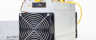
An FPGA (Field Programmable Gate Array) is cryptocurrency mining hardware that is very similar to an ASIC except for one key feature.
In the mining area, you can change your FPGA from Cryptonight mining to Lyra2z mining in seconds. This can also be done with processors and video cards, but for certain reasons the FPGA is much faster.
Certain FPGA boards are known to perform 100 times better than GPUs with the same power consumption. Depending on the algorithm, the FPGA may lag slightly or not lag behind the ASICs at all.
Material navigation:
Operating principle of FPGA chips
For mining on an FPGA, bitstream is written - chip firmware, which indicates how the FPGA should solve the problem necessary for mining a particular coin. Bitstreams are programmed in Verilog or VHDL.
FPGA chip is a semiconductor chip. Used in cases where the device is designed to perform logical operations such as and, or, nand and others.
That is, it is a microcircuit with repeating logical blocks connected in a circuit. They can be configured at your own discretion, taking into account the tasks.
FPGA-based equipment is initially designed for air cooling. With it, the operating temperature of the chip reaches 100 degrees. When operating chips under such conditions, one of the leading manufacturers, Xilinx, provides a three-month warranty. But with immersion cooling, the chip temperature does not exceed 80 degrees.
Thanks to this, the entire board and all the chips that are on it operate in ideal conditions. This significantly increases the lifespan of the chips and automatically increases the hash rate.
Pros of FPGA:
Disadvantages of FPGA:
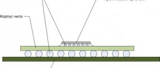
Signal input/output blocks.
FPGAs are widely used because they can be included in most computing device designs and can replace a large number of older chips. The prerequisite for this is a large number of IOB signal input/output blocks, customizable to various standards for the electrical connection of microcircuit inputs. In Fig. the structure of one IOB is shown.
The signal pin of the FPGA is called PAD. By setting it, you can connect an internal PULLUP resistor or a PULLDOWN resistor connected to the power bus or ground bus, respectively. These resistors provide open collector (drain) output mode for systems with different logic levels. The input signal from the PAD goes to the IBUF comparator, the response threshold of which is programmed for TTL, CMOS, PCI bus levels and many others, and can also be adjusted by setting the externally supplied voltage. To ensure a time shift of the signal relative to the front of the clock series, ensuring reliable reception of the signal into internal triggers, a special delay circuit can be included in the input signal circuit.
The output signal in the IOB is generated in a tristable OBUFT buffer, and its maximum current level is programmable in steps and can reach 20 mA. To provide high-speed I/O, the transmitted and received data bits, as well as the tristable buffer control signal, can be stored in flip-flops.
The new series of FPGAs provide adjustment of the input and output impedance of the PADs, as well as biphasic operation of pairs of PADs to achieve noise-resistant high-speed data transfer.
During diagnostics and debugging, in one of the configuration modes, the FPGA can be switched to the Boundary Scan mode. In this mode, all IOBs are chained together into one long shift register. By standard external control of this shift register via the JTAG interface, you can read pin states, send test signals, and configure the FPGA.
During the configuration period of the FPGA, in order to ensure that the devices connected to it do not function in an uncertain manner, the IOB outputs are turned off and they are usually set to the H level of a weak unit (Weak Keeper).
Evolution of mining equipment - from CPU, GPU, FPGA, ASIC
This led to the transition of mining to industrial scale - the use of GPUs (video cards). Video cards had tens of times greater hashing speed at a lower cost. A clear advantage of mining coins on both the CPU and GPU was the ability to switch from one to the other, depending on the market situation.
In 2011, some enthusiasts began searching for less power-consuming devices for mining, and found FPGAs. Farms with FPGA cards were many times more productive and energy efficient, but expensive and difficult to program. In 2013, the first ASICs appeared - designed for mining one coin, powerful and easy to use.
The economics of mining were changing. The main factors behind the changes include the bear market for cryptocurrencies and the ever-increasing difficulty of mining. Therefore, the hashing power and ease of use of the emerging ASICs determined their popularity.
The rise of ASICs has led to another problem - centralization or the so-called "51% attack" risk of many large coins, which forces developers to change hashing algorithms.
The big disadvantage of ASICs for miners is that if the hashing algorithm changes, mining with them will become impossible, since the calculation algorithm cannot be changed. All that remains is to buy an ASIC and hope that the investment will pay off before the coin mining algorithm changes or the difficulty of mining this coin increases to the skies.
GPU mining is still a workable option, but the high power consumption of video cards makes mining pointless in many regions where the cost of 1 kWh of electricity is above 7-12 cents in the current market situation. Of course, manufacturers of mining equipment are thinking about whether there is an alternative to ASICs and GPUs? We found a solution - we returned to FPGA chips.
Circuits for accelerating arithmetic operations.
In the ECLB, two LTs and two flip-flops are connected together through a fast-transfer circuit and two one-bit half-adders. These circuits make it possible to effectively implement multi-bit parallel adders, and on their basis - all kinds of counters and ALUs.
To minimize hardware and speed up the calculation of the multiplication operation, an additional bitwise product circuit is used.
It should be added that the new VirtexII series has 18 by 18 bit multipliers implemented in hardware.
Comparison of FPGA miners with ASIC and GPU
FPGA (Field Programmable Gate Array) or field programmable gate array is one of the types of FPGA (programmable logic integrated systems) - an integrated circuit that can be reconfigured for any complex computing tasks.
The first FPGAs for commercial use were developed in 1985, they were used in scientific computing, military electronics, telecommunications, video processing, medicine, industry, etc. FPGAs are still used in these areas today. In the field of cryptocurrency mining, FPGAs can be configured to mine different coins within a second.
Unlike the CPU and GPU, an FPGA card can be reprogrammed for the task being solved on it. One of the most important features of FPGAs for mining is reduced power consumption per unit of computing power.
If FPGAs are so versatile, then why haven’t they pushed ASICs out of the market yet? This equipment was not widely used for several reasons.
Reason one: FPGA is not easy to configure due to the flexibility and architecture of the card. They can be programmed to do anything, but this requires knowledge of unpopular low-level languages - Verilog or VHDL. And if the video card can be configured using the BIOS and the miner, then the FPGA board must be programmed from scratch, and this takes time.
The second reason stems from this reason – the appearance of ASICs on the market. The ASIC doesn't need to be configured, it's easy to use, and that's what most miners need. FPGAs are used to prototype ASICs, but programming them is the job of the manufacturer, not the miner.
However, with the increase in the number of ASICs in large mining pools, the so-called threat of a “51% attack” has appeared for various coins. Then the creators of these coins began to change algorithms in the fight for decentralization of the blockchain, as mentioned above.
FPGA vs ASIC
The first thing to note is that developing an FPGA is much easier. Unlike FPGAs, ASIC design starts with a completely empty table. This does not mean that everyone will set up a chip for mining at home. But if you have a base and read the experience of others (more on this below), the task is theoretically feasible.
On an FPGA you start with a large array of logic blocks, PLLs, on-chip RAMs, I/O buffers, (de)serializers, power distribution networks, etc., ASIC development yourself starts at an even lower level. This means that components must be purchased or manufactured as part of a library, or custom designed for the ASIC.
One ASIC production cycle can take several weeks (months), after which you need to integrate and test it. After testing, bugs are not fixed, it is too expensive.
ASIC technology provides higher speed and lower power consumption compared to FPGA. The differences in speed between the two methods are easily 10 times or more.
FPGA vs video cards (GPU)
GPUs are significantly more powerful than CPU's, both in power and hash/watt, but due to FGPA's inherent parallelism can be around 15x more efficient.
Overall, the takeaway from FPDAs is that they consume less power and can be reconfigured and designed by yourself if you're good with microelectronics. But they have:
Despite the higher price, ASIC will be more profitable. But for coins that are resistant to such development, you can try an FPGA miner.
FPGA architecture from Xilinx.
Xilinx is one of the founders of FPGAs and their largest manufacturers. Below is a brief description of the architectural features of the Virtex series FPGAs produced by this company. These features are inherited in the new FPGA series, as well as in the Spartan series, the chips of which are designed to replace custom VLSI in small- and medium-scale production of electronics products. In addition, the operating principles of the FPGA structural elements of this series are recognizable in the FPGA architectures of other manufacturers, such as Altera, Actel, Atmel.
Where can you buy FPGA in 2019?
The main FPGA manufacturers - Xilinx and Altera (Intel) - are located in the USA, which makes it more difficult to buy a card. Since there are only a few manufacturers of these cards, it is impossible for a retail buyer to purchase them directly.
Large miners in Europe and Asia can also order cards through the American company SQRL or the Cyprus company COMINO, but this also poses a number of difficulties, such as customs paperwork.
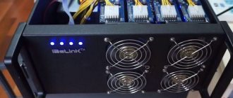
Another solution - CrystalCore based on FPGA Xilinx UltraScale Plus - is offered by engineers of the Belarusian company AETTECH. The equipment is a cell with an immersion liquid in which from three to nine FPGA chips and other electronic components that support the operation of these chips are immersed.
Logical table.
The role of the main logical element in the FPGA is played by a logic table (LT) or look-up table (LUT), which is a one-bit RAM with 16 cells. A unit is written in the LT at the address G3, G2, G1, G0 if the address code is a constituent of the unit of a given four-input logical function. For example, if a one is written at address 1,1,1,1, and zero at the other addresses, then the LT implements a four-input AND function. In Fig. shows an example of coding a four-input Exclusive OR function.
LT triggers are part of the programming shift register and their initial state is filled during the FPGA configuration period.