The Radeon RX 400 series has been a major commercial success for AMD's graphics division. After four years of agonizing wait, GPU manufacturers received the next generation technological process - 14/16 nm FinFET, and AMD, this time choosing GlobalFoundries as a chip contractor, introduced the Radeon RX 460, RX 470 and RX 480, covering the low and mid-range performance segments. Thanks to attractive prices, AMD managed to seriously compete with NVIDIA's GeForce 10 series in the corresponding price categories, but from a technical point of view, the Polaris family did not fully satisfy enthusiasts, since AMD's rival made much better use of the capabilities of the new process technology in terms of energy efficiency and frequency potential of the GPU.
Rumors that AMD is working on a deep revision of the Polaris line arose back in October last year - just a couple of months after the last representative of the 400 series - the Radeon RX 460 - went on sale. Indeed, the Radeon 500 series, according to the manufacturer, does not simply consist of rebranded Radeon 400 models, but is equipped with second-generation Polaris crystals, which combine an optimized design with mature 14 nm FinFET technology.
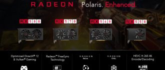
The new Radeon line is represented by four video cards with the indices RX 550, RX 560, RX 570 and RX 580, among which the flagship model based on the Polaris 20 GPU is the first to be tested.
Specifications
The Polaris 20 GPU is an updated version of the Polaris 10 core found in the Radeon RX 480. As a result, the composition of the computing units has not changed. Like Polaris 10, the fully functional version of Polaris 20 has 2304 shader ALUs, 144 texture mapping units and 32 ROPs, and the chip is connected to the RAM via a 256-bit bus with a bandwidth of 8 Gbps per pin.
Let us recall that from the point of view of microarchitecture, the Polaris series has a number of differences from previous AMD products based on GCN logic version 1.2 (the Fiji chip in the Radeon R9 Nano, R9 Fury and Fury X), among which an important place is occupied by color compression with a ratio of up to 8 :1, allowing more efficient use of RAM bus bandwidth. Among other optimizations of the internal structure of the GPU presented in GCN 1.3, we note the optimization of the geometry engine, which is capable of cutting off polygons of zero size or those without pixels in the projection at the early stages of the pipeline. The Compute Unit (the main GCN structure that combines shader ALUs and texture mapping units) has also been tuned in Polaris to improve its specific performance.
Functional innovations in Polaris include support for the half-bit number formats int16 and FP16, which are used in computational tasks that do not require more precise representation (such as machine learning).
The dedicated GPU codec allows hardware to encode and decode video in HEVC Main 10 and VP9 formats with resolutions up to 4K. The display controller supports signal output via DisplayPort 1.3/1.4 and HDMI 2.0b interfaces, as well as high dynamic range (HDR). You can get more detailed information about the GCN 1.3 architecture and Polaris chips in our Radeon RX 480 review.
The only change brought by the new version of the older core of the Polaris family, together with the optimized 14 nm FinFET process technology, is the GPU clock speed, which AMD, according to standard specifications, increased from 1266 MHz to the level that was achieved in the best samples of the Radeon RX 480 based original design printed circuit boards - 1340 MHz. The effective frequency of RAM chips is still 8 GHz, and the standard capacity is 4 or 8 GB. At the same time, AMD had to increase the standard thermal package of the video card from 150 to 185 W in order to give way to increased clock frequencies.
The Radeon RX 580 goes on sale at the same retail price as the Radeon RX 480: $199 for cards with 4 GB of RAM and $229 for 8 GB of RAM. AMD has set recommended prices for Russian sellers at 13,449 and 15,299 rubles. respectively.
| Manufacturer | AMD | |||
| Model | Radeon RX 470 | Radeon RX 480 | Radeon RX 570 | Radeon RX 580 |
| GPU | ||||
| Name | Polaris 10 | Polaris 10 | Polaris 20 XL | Polaris 20 XTX |
| Microarchitecture | GCN 1.3 | GCN 1.3 | GCN 1.3 | GCN 1.3 |
| Technical process, nm | 14 FinFET | 14 FinFET | 14 FinFET | 14 FinFET |
| Number of transistors, million | ||||
| Clock frequency, MHz: Base Clock / Boost Clock | 926/1206 | 1120/1266 | 1168/1244 | 1257/1340 |
| Number of shader ALUs | 2048 | 2304 | 2048 | 2304 |
| Number of texture mapping units | 128 | 144 | 128 | 144 |
| ROP number | 32 | 32 | 32 | 32 |
| RAM | ||||
| Bus width, bits | 256 | 256 | 256 | 256 |
| Chip type | GDDR5 SDRAM | GDDR5 SDRAM | GDDR5 SDRAM | GDDR5 SDRAM |
| Clock frequency, MHz (bandwidth per contact, Mbit/s) | 1650 (6600) | 2000 (8000) | 1750 (7000) | 2000 (8000) |
| Volume, MB | 4096 | 4096/8192 | 4096 | 4096/8192 |
| I/O bus | PCI Express 3.0 x16 | PCI Express 3.0 x16 | PCI Express 3.0 x16 | PCI Express 3.0 x16 |
| Performance | ||||
| Peak performance FP32, GFLOPS (based on maximum specified frequency) | 4940 | 5800 | 5059 | 6175 |
| Performance FP32/FP64 | 1/16 | 1/16 | 1/16 | 1/16 |
| RAM bandwidth, GB/s | 211 | 224 | 224 | 256 |
| Image output | ||||
| Image output interfaces | DL DVI, HDMI 2.0b, DisplayPort 1.3/1.4 | DL DVI, HDMI 2.0b, DisplayPort 1.3/1.4 | DL DVI, HDMI 2.0b, DisplayPort 1.3/1.4 | DL DVI, HDMI 2.0b, DisplayPort 1.3/1.4 |
| TDP, W | 120 | 150 | 150 | 185 |
| Suggested retail price (USA, excluding tax), $ | 169 (after reduction in autumn 2016) | 199/229 (at the time of release) | 169 | 199/229 |
| Recommended retail price (Russia), rub. | ND | 16,310 / 18,970 (at time of release) | 11 299 | 13 449 / 15 299 |
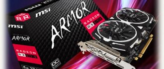
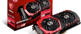
SAPPHIRE NITRO+ Radeon RX 580: technical specifications, design
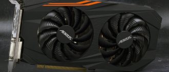
The Radeon RX 580 has been available in original designs from day one. Therefore, instead of a reference video card, which can only be seen at AMD presentations, we will study the new product using the example of the SAPPHIRE NITRO+ Radeon RX 580 accelerator. The powerful cooling system and circuit design of the board allowed the manufacturer to increase the GPU clock speeds relative to AMD reference specifications - up to 1411 MHz. At the same time, the second version of the BIOS, which can be activated by a switch on the end of the printed circuit board, contains even more aggressive settings with a maximum core frequency of 1450 MHz, although this feature is not indicated in the official characteristics of the device. There are two versions of the video card with 4 and 8 GB of RAM - this is the older (and most expensive) of them.
The design of the NITRO+ Radeon RX 580 cooling system follows the models that the company produced in the Radeon 400 generation, such as the NITRO+ Radeon RX 480. The large cooler casing protrudes beyond the area of the printed circuit board. Thus, part of the radiator located inside “hangs” over the edges and is blown right through by the fans. The back surface of the PCB is covered with a protective aluminum plate.
In the video card cooling system, a central copper block is connected to the fins by heat pipes, and two separate plates are pressed against the RAM chips and powerful VRM transistors. Due to the increased heat dissipation of the Radeon RX 580, the manufacturer has upgraded the radiator design compared to the NITRO+ RX 480, installing an additional fourth heat pipe and increasing the total area of the fins.
The air flow is created by a pair of fans with a diameter of 95 mm on double ball bearings. Because each fan is held in place by a single screw and connected via a connector, there's no need to remove the cooling shroud or unsolder any wires to remove them.
According to SAPPHIRE, a reinforced heatsink and new fan control circuitry have reduced noise by 12 dB under load. In addition, the Limited Edition NITRO+ RX 580 we received for testing comes with an additional pair of fans with clear blue glowing blades that can be installed in place of the standard black fans. The glowing SAPPHIRE logo on the side of the video card can be given any color using the proprietary SAPPHIRE TRIXX utility.
SAPPHIRE NITRO+ Radeon RX 580: board
The board's voltage converter is built according to a 6+1 phase scheme (for powering the GPU and RAM, respectively), not counting the PLL phase. The voltage on the GPU is controlled by the IR 3567B PWM controller, which video cards based on AMD chips have been using since the Radeon R9 290X. The power part of the circuit includes long-life polymer capacitors and chokes with Black Diamond 4 finned “micro-radiators”, which are 15% cooler compared to the previous iteration (according to the manufacturer).
The developers have changed the video output configuration that is standard for Polaris-based AMD video adapters, returning the DVI-D port and replacing one of the DisplayPort connectors with HDMI. Thus, you can simultaneously connect a screen with an HDMI interface and a virtual reality headset to the video card (all of them currently use HDMI).
⇡#Test stand, testing methodology
| Test bench configuration | |
| CPU | Intel Core i7-5960X @ 4 GHz (100 MHz × 40), constant frequency |
| Motherboard | ASUS RAMPAGE V EXTREME |
| RAM | Corsair Vengeance LPX, 2133 MHz, 4 × 4 GB |
| ROM | Intel SSD 520 240 GB + Crucial M550 512 GB |
| power unit | Corsair AX1200i, 1200 W |
| CPU cooling system | Thermalright Archon |
| Frame | CoolerMaster Test Bench V1.0 |
| Monitor | NEC EA244UHD |
| operating system | Windows 10 Pro x64 |
| Software for AMD GPUs | |
| All video cards | 22.19.147.0 WHQL |
| NVIDIA GPU software | |
| All video cards | GeForce Game Ready Driver 378.78 WHQL |
| Benchmarks: synthetic | |||
| Test | API | Permission | Full screen anti-aliasing |
| 3DMark Fire Strike | DirectX 11 (feature level 11_0) | 1920 × 1080 | Off |
| 3DMark Fire Strike Extreme | 2560 × 1440 | ||
| 3DMark Fire Strike Ultra | 3840 × 2160 | ||
| 3DMark Time Spy | DirectX 12 (feature level 11_0) | 2560 × 1440 | |
| Benchmarks: games | ||||
| Game (in order of release date) | API | Settings | Full screen anti-aliasing | |
| 1920 × 1080 / 2560 × 1440 | 3840 × 2160 | |||
| Crysis 3 + FRAPS | DirectX 11 | Max. quality. Start of the Swamp mission | MSAA 4x | Off |
| Metro: Last Light Redux, built-in benchmark | Max. quality | SSAA 4x | ||
| GTA V, built-in benchmark | Max. quality | MSAA 4x + FXAA + Reflection MSAA 4x | ||
| DiRT Rally, built-in benchmark | Max. quality | MSAA 4x | ||
| Rise of the Tomb Raider, built-in benchmark | DirectX 12 | Max. quality, VXAO off | SSAA 4x | |
| Tom Clancy's The Division, built-in benchmark | Max. quality, HFTS off | SMAA 1x Ultra + TAA: Supersampling | TAA: Stabilization | |
| Ashes of the Singularity, built-in benchmark | Max. quality | MSAA 4x + TAA 4x | Off | |
| DOOM | Vulkan | Max. quality. Foundry Mission | TSSAA 8TX | |
| Total War: WARHAMMER, built-in benchmark | DirectX 12 | Max. quality | MSAA 4x | |
| Deus Ex: Mankind Divided, built-in benchmark | Max. quality | MSAA 4x | ||
| Battlefield 1 + OCAT | Max. quality. Start of mission Through Mud and Blood | TAA | ||
| Benchmarks: video decoding, computing | |
| Program | Settings |
| DXVA Checker, Decode Benchmark, H.264 | Files 1920 × 1080p (High Profile, L4.1), 3840 × 2160p (High Profile, L5.1). Microsoft H264 Video Decoder |
| DXVA Checker, Decode Benchmark, H.265 | Files 1920 × 1080p (Main Profile, L4.0), 3840 × 2160p (Main Profile, L5.0). Microsoft H265 Video Decoder |
| LuxMark 3.1 x64 | Hotel Lobby Scene (Complex Benchmark) |
| Sony Vegas Pro 13 | Sony benchmark for Vegas Pro 11, duration - 65 s, rendering in XDCAM EX, 1920 × 1080p 24 Hz |
| SiSoftware Sandra 2016 SP1, GPGPU Scientific Analysis | Open CL, FP32/FP64 |
| CompuBench CL Desktop Edition X64, Ocean Surface Simulation | — |
| CompuBench CL Desktop Edition X64, Particle Simulation - 64K | — |
Test participants
The following video cards took part in performance testing:
- AMD Radeon R9 390X (1050/6000 MHz, 8 GB);
- AMD Radeon RX 480 (1266/8000 MHz, 8 GB);
- SAPPHIRE NITRO+ Radeon RX 580 (1340/8000 MHz, 8 GB);
- NVIDIA GeForce GTX 970 (1050/7010 MHz, 4 GB);
- NVIDIA GeForce GTX 1060 (1506/8000 MHz, 6 GB).
⇡#Performance: 3DMark
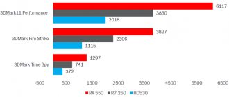
In synthetic benchmarks, the Radeon RX 580 scored 11% better than the RX 480 and outperformed rivals that its predecessor lost to, both the Radeon R9 390X and GeForce GTX 1060.
| 3DMark (Graphics Score) | ||||||
| Permission | AMD Radeon RX 580 (1340/8000 MHz, 8 GB) | AMD Radeon R9 390X (1050/6000 MHz, 8 GB) | AMD Radeon RX 480 (1266/8000 MHz, 8 GB) | NVIDIA GeForce GTX 970 (1050/7010 MHz, 4 GB) | NVIDIA GeForce GTX 1060 (1506/8000 MHz, 6 GB) | |
| Fire Strike | 1920 × 1080 | 13 904 | 13 165 | 12 310 | 11 117 | 12 890 |
| Fire Strike Extreme | 2560 × 1440 | 6 132 | 5 949 | 5 523 | 5 178 | 6 066 |
| Fire Strike Ultra | 3840 × 2160 | 3 032 | 2 988 | 2 701 | 2 467 | 2 891 |
| Time Spy | 2560 × 1440 | 4 202 | 4 134 | 3 953 | 3 511 | 4 107 |
| Max. | −1% | −6% | −16% | −1% | ||
| Average | −3% | −10% | −18% | −4% | ||
| Min. | −5% | −11% | −20% | −7% | ||
Architectural features of Polaris
What interesting things did users get with the release of the 4th generation GCN architecture and the Polaris graphics core?
Polaris architecture
All key blocks in the Polaris architecture have been updated (in order to increase its specific performance), namely:
- Computing blocks
- Geometry processor
- Command processing block
- Data caching system
- Memory controller
- Video stream encoding/decoding system
We won’t get into the detailed jungle of architectural updates, but here’s what’s interesting...
With revision 4 of the GCN architecture, the cards received support for modern HDMI 2.0a and display port 1.3/1.4 interfaces, which will allow you to display images in resolutions up to 8K. As well as high dynamic range (HDR).
Hardware has appeared to work with the h.265 codec. The dedicated GPU codec allows hardware to encode and decode video in HEVC Main 10 and VP9 formats with resolutions up to 4K.
When viewing and encoding a video in 4K 60FPS, you can take the load off the central processor.
Functional innovations in Polaris include support for half-digit number formats - INT16 and FP16, which are used in computational tasks that do not require more precise representation (such as machine learning).
Features of GCN 4th generation architecture
AMD itself highlights the following key properties of Graphics Core Next 4th:
- New instruction prefetch unit to reduce downtime of computational units
- New task scheduler that allows you to more efficiently distribute tasks between computing units
- New algorithms for memory compression and discarding polygons invisible in the frame, allowing to reduce the requirements for the amount of RAM, increase its useful bandwidth and avoid unnecessary time spent on calculations on parts of the image that are not visible in the final scene
- Color compression with ratios up to 8:1, allowing more efficient use of RAM bus bandwidth.
The comprehensive architecture optimization listed above, a larger number of computing units, and increased clock speeds provide performance at 6.2 TFLOPS (according to official data in reference models). And this was one of the reasons that AMD GСN 4th generation cards on Vulkan and DirectX12 are showing more and more performance in new and optimized projects, in comparison with direct competitors on Maxwell and Pascal architecture.
RX 580 vs GTX 1060
Since the release of the RX580 8Gb and GTX1060 6Gb video cards, the latter has noticeably outperformed the AMD card, but now the RX580 outperforms the 1060 in almost all games, showing performance gains every year. We have tests
And all thanks to the 4th generation GCN architecture, which had enormous computing resources, but did not show the best results in games, Direct 11 could not use its full potential.
All the computing power can be seen in the stated TFLOPS. Which have always been higher for AMD compared to similar gaming performance for NVIDIA.
⇡#Performance: games (1920 × 1080, 2560 × 1440)
The results of gaming tests in gentle graphics modes (1080p and 1440p) do not clearly speak in favor of the Radeon RX 580 or against it.
The difference between the Radeon RX 480 and RX 580 turned out to be slightly smaller than could be predicted from the nominal frequencies of the video cards - only 3-4%. In addition, despite the fact that the RX 580 sometimes provides higher frame rates than the Radeon R9 390X, on average the latter is 15% faster than the new product.
As for the latest generation video cards, at 1080p resolution the GeForce GTX 1060 has a 7% advantage over the Radeon RX 580, but at 1440p the Radeon RX 580 still achieved conditional parity with the GTX 1060. However, although the average advantage in favor of AMD's opponent is 3 %, in certain games, as a rule, one or another video card is significantly superior to its opponent.
| 1920 × 1080 | ||||||
| Full screen anti-aliasing | AMD Radeon RX 580 (1340/8000 MHz, 8 GB) | AMD Radeon R9 390X (1050/6000 MHz, 8 GB) | AMD Radeon RX 480 (1266/8000 MHz, 8 GB) | NVIDIA GeForce GTX 970 (1050/7010 MHz, 4 GB) | NVIDIA GeForce GTX 1060 (1506/8000 MHz, 6 GB) | |
| Ashes of the Singularity | MSAA 4x + TAA 4x | 24 | 45 | 24 | 29 | 28 |
| Battlefield 1 | TAA | 76 | 91 | 72 | 50 | 68 |
| Crysis 3 | MSAA 4x | 44 | 54 | 43 | 37 | 51 |
| Deus Ex: Mankind Divided | MSAA 4x | 25 | 30 | 24 | 19 | 22 |
| DiRT Rally | MSAA 4x | 57 | 58 | 54 | 46 | 65 |
| DOOM | TSSAA 8TX | 138 | 130 | 131 | 103 | 121 |
| GTA V | MSAA 4x + FXAA + Reflection MSAA 4x | 45 | 50 | 42 | 42 | 57 |
| Metro: Last Light Redux | SSAA 4x | 51 | 57 | 49 | 45 | 55 |
| Rise of the Tomb Raider | SSAA 4x | 35 | 34 | 32 | 21 | 35 |
| Tom Clancy's The Division | SMAA 1x Ultra + TAA: Supersampling | 60 | 55 | 58 | 42 | 56 |
| Total War: WARHAMMER | MSAA 4x | 39 | 44 | 38 | 33 | 43 |
| Max. | +88% | +0% | +21% | +26% | ||
| Average | +15% | −4% | −18% | +4% | ||
| Min. | −8% | −9% | −40% | −12% | ||
| 2560 × 1440 | ||||||
| Full screen anti-aliasing | AMD Radeon RX 580 (1340/8000 MHz, 8 GB) | AMD Radeon R9 390X (1050/6000 MHz, 8 GB) | AMD Radeon RX 480 (1266/8000 MHz, 8 GB) | NVIDIA GeForce GTX 970 (1050/7010 MHz, 4 GB) | NVIDIA GeForce GTX 1060 (1506/8000 MHz, 6 GB) | |
| Ashes of the Singularity | MSAA 4x + TAA 4x | 19 | 34 | 17 | 20 | 21 |
| Battlefield 1 | TAA | 61 | 64 | 59 | 37 | 53 |
| Crysis 3 | MSAA 4x | 27 | 35 | 24 | 23 | 32 |
| Deus Ex: Mankind Divided | MSAA 4x | 16 | 19 | 16 | 10 | 14 |
| DiRT Rally | MSAA 4x | 41 | 43 | 39 | 36 | 45 |
| DOOM | TSSAA 8TX | 89 | 87 | 85 | 63 | 77 |
| GTA V | MSAA 4x + FXAA + Reflection MSAA 4x | 31 | 35 | 29 | 26 | 39 |
| Metro: Last Light Redux | SSAA 4x | 28 | 31 | 27 | 28 | 32 |
| Rise of the Tomb Raider | SSAA 4x | 22 | 22 | 20 | 13 | 21 |
| Tom Clancy's The Division | SMAA 1x Ultra + TAA: Supersampling | 44 | 41 | 42 | 31 | 40 |
| Total War: WARHAMMER | MSAA 4x | 26 | 30 | 26 | 20 | 28 |
| Max. | +79% | +0% | +5% | +23% | ||
| Average | +15% | −5% | −22% | +3% | ||
| Min. | −7% | −11% | −41% | −13% | ||
Assassin's Creed Odyssey (2018)
I7 4770K + RX 580 in Assassin's Creed Odyssey (2018)
FPS readings:
- 1% Low – 48
- AVG - 54
Assassin's Creed Odyssey expected a much worse result. But even here the RX 580 with I7 4770k showed excellent results. The average FPS is 54. This would be normal, but knowing the optimization of this game for Nvidia, the RX 580 surprised.
⇡#Performance: games (3840 × 2160)
The Radeon RX 580 is clearly not designed for 4K resolution, even without full-screen antialiasing. A rare game with such settings reaches 30 FPS on Polaris 20. At the same time, it is in the 2160p mode that the ratio of results between video cards is most favorable for the new product. The Radeon RX 580 is 8% better than the GeForce GTX 1060 (let the latter remain strong in certain games), and the Radeon R9 390X's advantage has been reduced to 8%.
| 3840 × 2160 | ||||||
| Full screen anti-aliasing | AMD Radeon RX 580 (1340/8000 MHz, 8 GB) | AMD Radeon R9 390X (1050/6000 MHz, 8 GB) | AMD Radeon RX 480 (1266/8000 MHz, 8 GB) | NVIDIA GeForce GTX 970 (1050/7010 MHz, 4 GB) | NVIDIA GeForce GTX 1060 (1506/8000 MHz, 6 GB) | |
| Ashes of the Singularity | Off | 37 | 44 | 36 | 20 | 26 |
| Battlefield 1 | 37 | 40 | 36 | 23 | 29 | |
| Crysis 3 | 20 | 24 | 18 | 16 | 21 | |
| Deus Ex: Mankind Divided | 17 | 19 | 17 | 10 | 15 | |
| DiRT Rally | 27 | 28 | 25 | 19 | 29 | |
| DOOM | 45 | 49 | 42 | 33 | 40 | |
| GTA V | 29 | 29 | 29 | 23 | 31 | |
| Metro: Last Light Redux | 26 | 29 | 25 | 24 | 28 | |
| Rise of the Tomb Raider | 26 | 27 | 25 | 13 | 25 | |
| Tom Clancy's The Division | TAA: Stabilization | 26 | 26 | 26 | 15 | 22 |
| Total War: WARHAMMER | Off | 24 | 24 | 24 | 17 | 22 |
| Max. | +20% | +0% | −7% | +9% | ||
| Average | +8% | −3% | −32% | −7% | ||
| Min. | +0% | −10% | −50% | −30% | ||
Battlefield V (2018)
I7 4770K + RX 5700 XT in Battlefield V (2018)
FPS readings:
- 1% Low – 55
- AVG - 69
In Battlefield V, the emphasis is on the video card. RX 580 is 100% loaded. Average FPS is 69FPS. Excellent result.
⇡#Performance: video decoding
Polaris 20 has exactly the same multimedia unit as Polaris 10, so the difference in video stream decoding speed between video cards comes down to the ratio of their clock frequencies.
The Radeon RX 580, like its predecessor RX 480, is comparable to representatives of NVIDIA's Maxwell architecture in the H.264 test, but Pascal chips have incomparably higher throughput - in decoding both H.264 and HEVC format (H.265) .
Note: since decoders within the same GPU line usually do not differ, the diagrams show one device from each family (or more if this rule is violated).
Performance: Compute
The role of video cards in modern games and the potential of the RX 580
As time went on, video cards began to perform more and more work in games that had previously been performed by the processor; now the video card calculates a significant part of physics, geometry intersections, geometry deformation calculations, and much more.
And all this is done by the video card in parallel with the work of rendering based on shadows and light, coloring the picture.
And this work has become more complex in recent years.
All this led to the need to create better APIs that work with graphics at a lower level. Allowing graphics threads to be occupied by more heterogeneous tasks in parallel.
The requirements for video cards have become more stringent.
Now I load almost all tasks onto the video card, since the processor performs them much more slowly.
With each release of new applications and games, new APIs were required that, through lower communication with the graphics chip, could use the large computing resources of the video card. At the moment, DirectX 12 and Vulcan allow you to make optimal use of the video card's power.
And as we said earlier, video cards from AMD have significantly greater computing power compared to their competitors. And the 4th generation GCN architecture itself turned out to be more optimized for complex tasks.
Over time, more games began to use the new API. And the more adaptable RX 580 received more profit from this.
Here AMD once again demonstrates its ability to make a product with a foundation for the future, for which the industry was not unprepared at the time the architecture was released.
It’s a familiar story with the FX processor, which every year and the release of more and more optimized games for multi-threading has long left all its competitors from 2011 to 2015 far behind. And which at one time was hated by everyone who did not understand the peculiarities of its operation and overclocking.
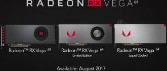
You can also recall video cards based on the Vega architecture, which have already been replaced by the more progressive RDNA architecture, which has absorbed and combined the best solutions of Polaris and Vega, as well as removing their shortcomings, not to mention a number of new revolutionary solutions (where would AMD be without revolution and potential) .
Looking ahead, I will say that the combination of the overclocked FX8350 and the overclocked RX580 in terms of price/performance ratio is practically unmatched in modern heavy games. Especially considering the ridiculous prices on the secondary market for these components. Although the surplus RX580 is still sold on store shelves, it is much more interesting to buy it on the used market, and buy a new one with the RX 5500 XT or, if possible, the RX 5600 XT, but this card is on a completely different level.
⇡#Clock speeds, power consumption, temperature, overclocking
To understand how the optimization of the 14 nm FinFET process technology in Polaris 20 affected the frequency potential and energy efficiency of the GPU compared to Polaris 10, it is worth comparing the Radeon RX 580 not with the reference video card, on the example of which we got acquainted with the Radeon RX 480 last year, but with a device of the original design - SAPPHIRE NITRO+ Radeon RX 480. Like other manufacturers who abandoned the reference design, SAPPHIRE allowed Polaris 10 to be seen in a favorable light, providing more efficient cooling and overclocking potential not available in earlier Radeon RX 480 samples.
Like its predecessor in the NITRO+ series, the Radeon RX 580 from SAPPHIRE supports the maximum GPU frequencies set by both BIOS versions - 1410 and 1450 MHz under gaming load. At the same time, when we reduced the frequency to the reference 1340 MHz, the supply voltage at the core did not exceed 1.15 V, while the NITRO+ Radeon RX 480 at its standard frequency of 1342 MHz showed values up to 1.175 V.
However, a system with an RX 580 on board has 12-16 W more power than the RX 480 (in FurMark and Crysis 3 tests, respectively). A possible reason is the power limit built into the SAPPHIRE NITRO+ Radeon RX 580 BIOS, since the video card is designed for higher frequencies than 1340 MHz, while for the NITRO+ RX 480 1342 MHz is the standard limit. As a result, the GPU supply voltage, which fluctuates at a high frequency in AMD GPUs, reaches its maximum more often.
Since the RX 580 received a 35 W higher TDP than the RX 480 (185 versus 150 W), the advantage of the main rival of the new product, the GeForce GTX 1060, in energy efficiency becomes more obvious than ever. The GTX 1060 delivers 60W less system power than the RX 580, reflecting the difference in the specifications of both cards (the GTX 1060 has a TDP of 120W).
In the BIOS, the NITRO+ RX 580 also differs from the NITRO+ RX 480 in the settings of the cooling system: if the NITRO+ RX 480 spins the cooler impellers up to 2016 rpm, then the RX 580 is content with 1322 rpm. However, this did not significantly affect the GPU temperature under load - the difference was only 4 °C.
The 1411 MHz frequency, which is standard for the NITRO+ RX 580, is beyond the capabilities of most Radeon RX 480 units with air cooling, but the manufacturer had to leave a reserve for further overclocking by the user. Remembering the modest overclocking capabilities of the Polaris 10, we did not expect a significant increase in frequencies, but the NITRO+ RX 580 presented a pleasant surprise. With a power limit of 150% and maximum speed of the cooling system, the graphics processor reached a frequency of 1500 MHz.
The bad news is that the Polaris 20 supply voltage in this case reaches 1.3563 V, and we did not increase it manually - this is what the video card automatics ordered. In any case, these are large numbers even for GPUs built using the 28 nm process technology, not to mention the 14 nm FinFET, and we are not sure that constant operation of the device with such operating parameters is safe for it.
The RAM overclocked not as successfully as the GPU, reaching only 8700 MHz effective frequency. Even increasing the voltage on the microcircuits from 0.95 to 1.2 V did not allow us to cross this mark.
Not surprisingly, the overclocked NITRO+ Radeon RX 580 develops the maximum power of all test participants, including even the Radeon R9 390X. Fortunately, the video card cooler effortlessly copes with the removal of additional heat. Even though we always run the impellers at maximum speed for overclocking, users will certainly be able to find a compromise between GPU temperature and cooling system noise.
Features of Polaris chips
Polaris architecture chips are built on the 14 nm FinFET process.
AMD described the appearance of the new architecture as a historic leap in performance per watt. In which, without a doubt, the transition to 14 hm played an important role.
To be more precise, AMD claims that the transition from 28 nm to 14 nm increased specific performance by 1.7 times, and architecture optimization brought the ratio to 2.8 times.
The RX 580 is based on the second-generation Polaris processor Polaris 20, which is an updated version of the Ploaris 10 core. Essentially, the RX580 is an overclocked RX480 with higher-quality crystals.
⇡#Performance: overclocking
In synthetic tests, overclocking improved the video card's results by 7–8%. In games, the frame rate also increased by 8-9%, depending on the resolution.
| 3DMark (Graphics Score) | |||
| Permission | AMD Radeon RX 580 (1340/8000 MHz, 8 GB) | SAPPHIRE NITRO+ Radeon RX 580 (1500/8700 MHz, 8 GB) | |
| Fire Strike | 1920 × 1080 | 13 904 | 14 962 |
| Fire Strike Extreme | 2560 × 1440 | 6 132 | 6 594 |
| Fire Strike Ultra | 3840 × 2160 | 3 032 | 3 250 |
| Time Spy | 2560 × 1440 | 4 202 | 4 540 |
| Max. | +8% | ||
| Average | +8% | ||
| Min. | +7% | ||
| 1920 × 1080 | |||
| Full screen anti-aliasing | AMD Radeon RX 580 (1340/8000 MHz, 8 GB) | AMD Radeon RX 580 (1500/8700 MHz, 8 GB) | |
| Ashes of the Singularity | MSAA 4x + TAA 4x | 19 | 21 |
| Battlefield 1 | TAA | 76 | 83 |
| Crysis 3 | MSAA 4x | 44 | 48 |
| Deus Ex: Mankind Divided | MSAA 4x | 25 | 28 |
| DiRT Rally | MSAA 4x | 57 | 62 |
| DOOM | TSSAA 8TX | 138 | 149 |
| GTA V | MSAA 4x + FXAA + Reflection MSAA 4x | 45 | 49 |
| Metro: Last Light Redux | SSAA 4x | 51 | 55 |
| Rise of the Tomb Raider | SSAA 4x | 35 | 37 |
| Tom Clancy's The Division | SMAA 1x Ultra + TAA: Supersampling | 60 | 65 |
| Total War: WARHAMMER | MSAA 4x | 39 | 43 |
| Max. | +12% | ||
| Average | +9% | ||
| Min. | +6% | ||
| 2560 × 1440 | |||
| Full screen anti-aliasing | AMD Radeon RX 580 (1340/8000 MHz, 8 GB) | AMD Radeon RX 580 (1500/8700 MHz, 8 GB) | |
| Ashes of the Singularity | MSAA 4x + TAA 4x | 24 | 25 |
| Battlefield 1 | TAA | 61 | 65 |
| Crysis 3 | MSAA 4x | 27 | 29 |
| Deus Ex: Mankind Divided | MSAA 4x | 16 | 17 |
| DiRT Rally | MSAA 4x | 41 | 44 |
| DOOM | TSSAA 8TX | 89 | 95 |
| GTA V | MSAA 4x + FXAA + Reflection MSAA 4x | 31 | 35 |
| Metro: Last Light Redux | SSAA 4x | 28 | 31 |
| Rise of the Tomb Raider | SSAA 4x | 22 | 25 |
| Tom Clancy's The Division | SMAA 1x Ultra + TAA: Supersampling | 44 | 49 |
| Total War: WARHAMMER | MSAA 4x | 26 | 28 |
| Max. | +14% | ||
| Average | +8% | ||
| Min. | +4% | ||
| 3840 × 2160 | |||
| Full screen anti-aliasing | AMD Radeon RX 580 (1340/8000 MHz, 8 GB) | AMD Radeon RX 580 (1500/8700 MHz, 8 GB) | |
| Ashes of the Singularity | Off | 37 | 41 |
| Battlefield 1 | 37 | 41 | |
| Crysis 3 | 20 | 23 | |
| Deus Ex: Mankind Divided | 17 | 18 | |
| DiRT Rally | 27 | 28 | |
| DOOM | 45 | 50 | |
| GTA V | 29 | 31 | |
| Metro: Last Light Redux | 26 | 28 | |
| Rise of the Tomb Raider | 26 | 27 | |
| Tom Clancy's The Division | TAA: Stabilization | 26 | 27 |
| Total War: WARHAMMER | Off | 24 | 25 |
| Max. | +15% | ||
| Average | +8% | ||
| Min. | +4% | ||
Comparison RX 580 8GB vs 1660 Super
Let's see the card in action and compare it with the GTX 1660 Super, and then I'll talk about the operating experience and some interesting features. The test will include only 3 games that will not rely on the processor.
We have many tests of this video card on our website, FX 8350 with RX 580, AMD FX 6300 with RX 580 8GB.
You can also watch the full test with a video card from NVIDIA, FX 8350 with GTX 1660 Super.
Witcher 3: Wild Hunt
Resident Evil 2 Remake
Metro Exodus
Test results RX 580 vs 1660 Super
The test results show that the AMD card is inferior to the more expensive GTX 1660 Super by about 20-30%, depending on the game, the price difference is 30%, and let’s not forget that there is a 3-year difference between the cards.
⇡#Conclusions
Standard practice for GPU manufacturers is to use GPUs familiar to buyers in a new series of video adapters, when the next generation chips are not yet ready for production, and the “old” chips still meet the requirements for speed and energy efficiency. And although from a practical point of view such a “rebranding” is completely justified, it is often a sign of technical difficulties or a lack of resources at the company, and certainly does not find a response in the hearts of computer hardware enthusiasts. Both of these fully apply to the latest rebranding of AMD graphics accelerators, when the set of processors on which the Radeon 200 series was based almost completely moved into the Radeon 300 series.
However, the raison d'être of the Radeon 500 line isn't to dust off Polaris chips. This time, AMD responded to criticism of the Radeon 400 series video cards by optimizing the chip design and 14 nm FinFET process technology, which is used to produce Polaris. At the moment, we had the opportunity to study only the flagship model of the Radeon 500 family, but we can repeat with confidence that this is not just a relabeled version of the Radeon RX 480, but a video card with a completely different frequency potential. Although the Polaris 20 chip still cannot compete in this parameter with modern NVIDIA products, even this increase in frequencies, combined with the “wide” GCN 1.3 architecture, finally allowed AMD to present an equal rival to the GeForce GTX 1060, while maintaining the attractive price level that it set Radeon 400 series.
At the same time, the capabilities that AMD had at its disposal thanks to the second generation Polaris silicon were fully used to increase clock speeds, and the graphics card power increased accordingly. The GCN architecture still cannot compete with Pascal in terms of energy efficiency, and AMD, as it already did with the Radeon 300 series, relied on performance instead of a compromise solution that could bring the Radeon RX 580 closer to the GeForce GTX 1060 in terms of power consumption, but not bridge the productivity gap.
In addition, although the average results in gaming tests at 1440p resolution have established a precarious parity between the Radeon RX 580 and the GeForce GTX 1060, AMD's rival maintains a confident advantage in many games. At the same time, most of our test clip already consists of games for DirectX 12, so individual failures of the Radeon RX 580 can no longer be attributed to the potential of the architecture, which the previous version of the Microsoft API cannot reveal. Finally, even though AMD positions the Radeon RX 580 as a video card for resolutions of 1080p and higher, it is in Full-HD mode rather than in 1440p that the new product provides the most comfortable frame rate, and here the GTX 1060 is the undisputed leader in its price category among new generation accelerators.
Thus, the updated GPU made the Radeon RX 580 a more profitable alternative to the GeForce GTX 1060 than the RX 480, but the essence of AMD’s offer has not changed: the older Polaris still captivates not with absolute performance, but with a lower price (often), 8 GB of memory ( in older versions) and, by the way, the ability to combine two GPUs in one system, which the GTX 1060 (in all cases, except for selected games) lacks.
Polaris chip history and positioning
More than three years have passed since the release of the Polaris architecture, and AMD is moving to the new RDNA and RDNA 2 architecture. The RX 580 was replaced by the RX 5500 XT on the RDNA architecture with NAVI chips, and soon we will see a replacement with RDNA 2.
But how does Polaris, introduced to the world in 2016, fare now?
These chips were supposed to fill the most massive productive segments of the discrete GPU market up to $300 and impose serious competition on NVIDIA on Maxwell and Pascal architecture. Which they did very well. And the RX 480, RX 580 and RX 590 cards show better and better results every year (relative to their direct competitors, of course). We will also discuss this phenomenon.
And Vega chips were supposed to supplant NVIDIA in the more productive video card segment.
Thorough check of the used video card for performance.